
In precision analog design, the difference between a good prototype and a market-ready product often hinges on microvolt-level accuracy. The MAX74821 datasheet reveals a device engineered for exactly this challenge, boasting sub-50µV offset voltage and 0.25 pA input bias current. For US engineers facing stringent noise budgets in sensor interfaces, understanding these specific metrics is no longer optional—it’s critical for signal integrity.
Architectural Overview: Dual Rail-to-Rail CMOS Design
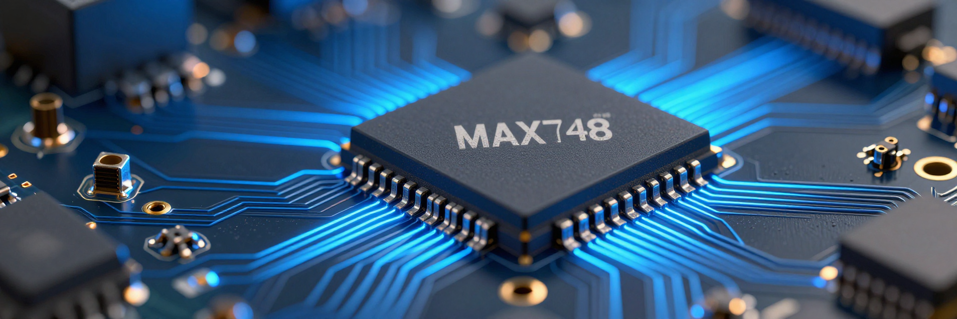
You will find that the MAX74821 integrates two independent operational amplifiers within a single package, optimizing board space without compromising channel isolation. This dual-channel architecture supports single-supply operation from 3.3 V to 5 V, making it highly versatile for modern low-power systems.
Single-Supply Operation & Input/Output Topology
The rail-to-rail input/output (RRIO) topology allows you to utilize the full dynamic range of your supply voltage. Unlike traditional op-amps that require headroom penalties, this design ensures signal swing extends nearly to the supply rails. Furthermore, the CMOS input stage provides extremely high impedance, which is essential when interfacing with high-resistance sensors like piezoelectric elements or photodiodes.
Power Efficiency vs. Performance Trade-offs
With an operating supply current of just 1 mA per channel, this component offers significant power savings compared to bipolar alternatives. If you are designing battery-powered IoT devices, this efficiency directly translates to extended runtime. You can achieve high performance without draining your power budget, a critical balance in portable electronics.
Critical Precision Metrics from the Datasheet
To ensure your system meets strict accuracy requirements, you must scrutinize the core specifications listed in the MAX74821 specs. These parameters define how well the amplifier preserves signal fidelity under varying conditions.
Offset Voltage & Drift Characteristics
The datasheet tables highlight a very low input offset voltage, typically under 50 µV. This minimizes DC error accumulation in your measurement chain. Additionally, the temperature drift coefficient is optimized to maintain stability across industrial temperature ranges. While zero-drift architectures exist, the MAX74821 offers a competitive edge by providing sufficient precision without the complexity and cost associated with chopper-stabilized designs.
Noise Density & CMRR Performance
When analyzing typical application graphs, you will observe low input voltage noise density, which is vital for high-resolution data acquisition. With an 85 dB Common Mode Rejection Ratio (CMRR), the device effectively suppresses common-mode interference, enhancing differential signal accuracy. For instance, in a 16-bit ADC front-end, calculating the total integrated noise ensures your Signal-to-Noise Ratio (SNR) remains above 90 dB, preserving least significant bit (LSB) integrity.
Dynamic Response & Bandwidth Analysis
Beyond static precision, you need to consider how the amplifier handles changing signals. The frequency response characteristics dictate whether your circuit can track fast-moving inputs without distortion.
Gain Bandwidth Product & Slew Rate Limits
The 10 MHz Gain Bandwidth Product (GBW) specification implies that as you increase closed-loop gain, available bandwidth decreases proportionally. Simultaneously, the 5 V/µs slew rate determines the maximum undistorted output frequency for large-signal swings. Refer to the table below for quick mapping:
| Closed-Loop Gain | Small-Signal Bandwidth | Max Frequency (Large Signal) |
|---|---|---|
| 1 V/V | ~10 MHz | ~150 kHz |
| 10 V/V | ~1 MHz | ~15 kHz |
| 100 V/V | ~100 kHz | ~1.5 kHz |
Phase Margin & Stability Considerations
The datasheet confirms robust capacitive load driving capabilities, reducing the risk of oscillation. However, when interfacing with long cables or heavy loads, you should implement small series resistors at the output. This compensation network isolates the capacitive load from the feedback loop, ensuring phase margin remains sufficient for stable operation.
Practical Implementation Scenarios
Translating theoretical specs into real-world circuits requires attention to layout and application context. Here is how you can leverage the MAX74821 in common designs.
Sensor Signal Conditioning Circuit Design
For thermocouple or strain gauge applications, configure the amplifier in a non-inverting topology to maximize input impedance. Pay close attention to PCB layout; minimize parasitic capacitance at the input pins by keeping traces short and using ground planes wisely. This prevents unwanted high-frequency noise coupling into sensitive microvolt-level signals.
Reference Buffering & Active Filter Applications
You can also deploy this op-amp as a precision reference buffer. Its low output impedance ensures stable voltage delivery to downstream converters, even under varying load conditions. Alternatively, its high input impedance makes it ideal for building second-order Sallen-Key filters, allowing you to shape signal bandwidth precisely without loading the source circuit.
Key Takeaways
- The MAX74821 delivers sub-50µV offset voltage, ensuring high DC accuracy for precision sensor interfaces.
- Rail-to-rail I/O and 1 mA/channel current consumption optimize dynamic range and power efficiency for battery-operated devices.
- A 10 MHz GBW and 85 dB CMRR support robust AC performance and effective noise rejection in mixed-signal systems.
Frequently Asked Questions
What is the primary advantage of the MAX74821 over standard op-amps?
The main advantage lies in its combination of rail-to-rail operation, ultra-low input bias current (0.25 pA), and low quiescent current. This makes it superior for high-impedance sensor applications where leakage currents would otherwise cause significant measurement errors in standard bipolar op-amps.
How does the MAX74821 handle noise in high-gain configurations?
While gain amplifies both signal and noise, the MAX74821’s low input voltage noise density helps maintain a favorable SNR. To further mitigate noise, use proper filtering techniques and keep input traces short to avoid picking up environmental electromagnetic interference during high-gain amplification stages.
Is external compensation required for stability with capacitive loads?
Generally, no external compensation is needed for moderate capacitive loads due to its inherent stability. However, for very large capacitive loads or long cable runs, adding a small series resistor (e.g., 10–50 Ω) at the output can isolate the capacitance and prevent potential oscillations.
What is the typical supply current consumption of the MAX74821?
The MAX74821 consumes approximately 1 mA per channel, making it highly efficient for battery-operated devices compared to traditional bipolar alternatives.