
The MAX74821ARMZ delivers microvolt-level offset, sub-picoamp input bias, a 10 MHz GBW, a 2.7–5.5 V operating range, and ≈1 mA quiescent current — a compact combination that favors precision, low-noise, and low-power front-end designs. This snapshot explains why the device is attractive for sensor interfaces and ADC drivers when small offset and low drift matter.
This report summarizes key items from the official datasheet, analyzes real-world implications for design, and gives practical validation and selection guidance engineers can apply during prototype and pre-production stages.
1 — MAX74821ARMZ at a glance: key specs & package (Background)
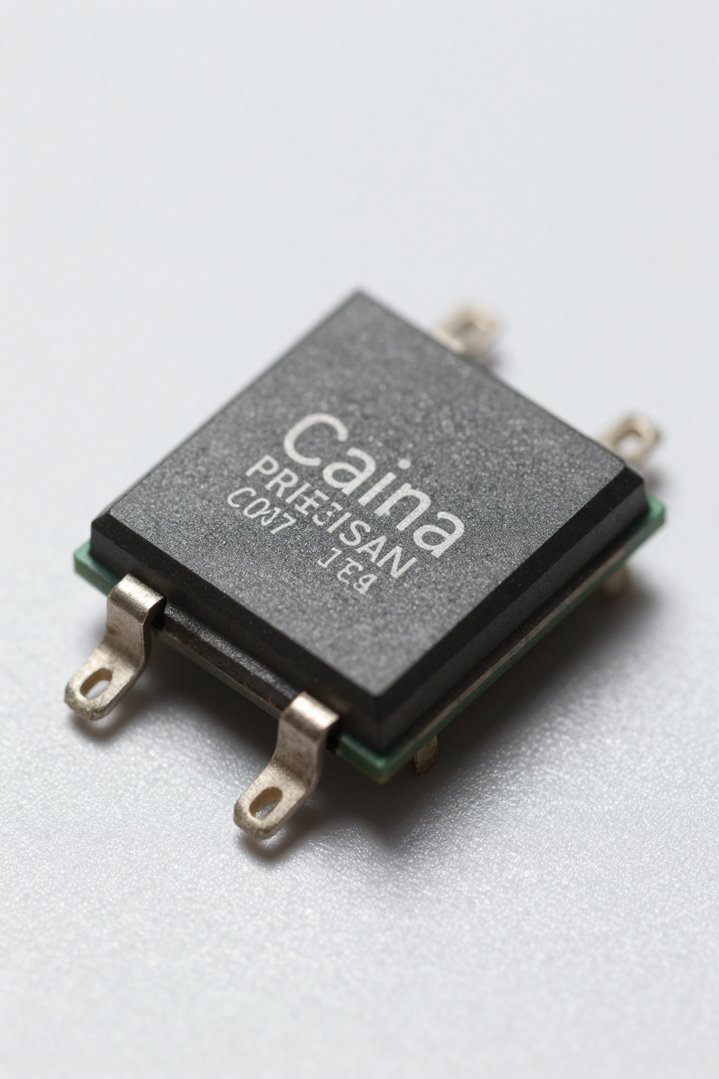
Key electrical highlights (what to list)
Point: Core specifications define suitability for precision front-ends. Evidence: Typical on-chip metrics include microvolt-class input offset (typical), sub-pA input bias, low voltage/current noise, 10 MHz GBW, rail-to-rail I/O, 2.7–5.5 V supply, and ~1 mA quiescent. Explanation: These specifications give a baseline for error budgeting and thermal/power trade-offs when selecting the part for low-drift, low-noise applications.
Package, pinout and ordering notes
Point: Package and padout affect layout and thermal performance. Evidence: The part comes in a small-leadframe package with multiple pins and exposed pad options; footprint density requires precise solder-mask and thermal-via planning. Explanation: Tight pad spacing demands careful land-pattern adherence and thermal vias beneath the exposed pad to limit temperature rise and maintain low-noise behavior in compact PCBs.
2 — Electrical performance deep-dive: offsets, noise, and DC characteristics (Data analysis)
Input-related specs and their design impact
Point: Input offset, drift, and bias set the DC error floor. Evidence: With microvolt-level offset and sub-pA bias, error contribution in a µV-level measurement chain can be dominated by offset and resistor-induced bias currents. Explanation: In high-impedance sensor interfaces, use low-leakage layout techniques, Kelvin sensing, and periodic offset calibration or digital trimming to suppress cumulative errors to the sub-µV range.
Noise profile and DC error budgeting
Point: Voltage noise density and bandwidth determine RMS noise. Evidence: Compute RMS noise as en_rms = en * sqrt(BW). Example: at 4 nV/√Hz and a 1 kHz bandwidth, en_rms ≈0.13 µV RMS. Explanation: Match source impedance to the amplifier's noise optimum; prefer this amplifier for low-source-impedance sensors where voltage noise dominates, and consider alternatives if source resistance is very high and current noise becomes limiting.
3 — Dynamic performance: bandwidth, slew rate, and stability (Data analysis)
AC specs: GBW, phase margin, and closed-loop behavior
Point: GBW and phase margin set closed-loop bandwidth and transient stability. Evidence: With a 10 MHz GBW, expect closed-loop bandwidth ≈GBW/closed-loop gain (for example, ≈1 MHz at gain of 10). Explanation: Check phase-margin notes in the official documentation and leave margin for parasitics; unity and low-gain configurations may need output loading and compensation considerations to avoid peaking or oscillation.
Slew rate, settling time, and capacitive loads
Point: Slew limits define large-step performance and ADC settling. Evidence: Slew-rate behavior limits how fast the output can change for large amplitude steps and affects settling to within ADC LSBs. Explanation: For ADC-driving roles, budget time for slew-dominated regions, add small series output resistors to isolate capacitive loads, and test settling to required resolution (e.g., 16–18 bits) under realistic source and cable loads.
4 — Power, supply range, and thermal considerations (Method / practical guidance)
Supply specs and power budgeting
Point: Supply range and quiescent current dictate power usage. Evidence: The official datasheet lists a 2.7–5.5 V operating range and ≈1 mA quiescent current. Explanation: For single-supply designs, power ≈VCC×Iq (at 5 V and 1 mA → 5 mW). For battery-powered systems, estimate battery life from Iq; in dual-supply topologies, account for both rails' currents and headroom requirements when choosing regulators and power sequencing.
Thermal limits, derating, and PCB layout tips
Point: Thermal impedance and copper area control die temperature under load. Evidence: Small packages require copper pour and thermal vias to spread dissipated power. Explanation: Use exposed-pad soldering, wide ground pours, and thermal vias to keep junction temperatures low; derate near maximum ambient limits and verify with thermal simulation when drive and ambient push dissipation above a few tens of mW.
5 — Typical application circuits & design recommendations (Method / guide)
Recommended configurations (gain stages, sensor front-ends, ADC buffers)
Point: Three common topologies leverage the part's strengths. Evidence: Low-noise preamp (low R values, shielding), precision buffer to ADC (unity or low gain with source isolation), and single-supply sensor amplifier (rail-to-rail I/O). Explanation: Use resistor values in the 1 kΩ–100 kΩ range depending on noise/impedance trade-offs, and include input protection (series R/clamp) when sensors may exceed inputs.
Practical layout and decoupling checklist
Point: Layout rules preserve low-bias and low-noise performance. Evidence: Decouple supply pins with a 0.1 µF ceramic close to the package and a 1 µF bulk nearby; route input traces short and guarded. Explanation: Implement guard rings tied to low-impedance reference, keep analog and digital grounds separate until a single-point tie, and avoid routing noisy traces near high-impedance inputs to prevent bias and noise degradation.
6 — Bench validation: test procedures and expected results (Method / guide)
Recommended test setups and measurement steps
Point: Reproducible tests validate datasheet claims. Evidence: Use a low-noise power supply, calibrated DMM, low-noise preamp/spectrum analyzer, and 100 MHz oscilloscope. Explanation: Measure offset with shorted inputs and high-resolution DMM, bias by measuring input offset under high-impedance source, noise via FFT with known bandwidth, GBW via network or transient step methods, and slew by fast step inputs into recommended load.
Interpreting results vs. datasheet values
Point: Measured deviations have known causes. Evidence: Differences often arise from test bandwidth, temperature, layout leakage, and measurement loading. Explanation: Reconcile by matching datasheet test conditions, reduce parasitics, improve grounding, and re-run tests; if offset/noise exceed expectations, inspect soldering, contaminants, and input protection networks.
7 — Application examples & selection checklist (Case studies + action)
Realistic application scenarios
Point: Practical examples show fit and trade-offs. Evidence: Use cases include precision thermistor amplifiers (low offset), low-current sensor interfaces (low bias), and ADC front-ends (low noise plus rail-to-rail I/O). Explanation: For each, adjust resistor values, add filtering for bandwidth control, and validate drift and PSRR under expected temperature and supply conditions.
Buy/use decision checklist
Point: A concise checklist reduces redesign risk. Evidence: Evaluate offset and drift, noise vs source impedance, GBW vs required closed-loop bandwidth, supply range and thermal limits, and prototype validation steps. Explanation: Perform the bench tests above, confirm package footprint and thermal plan, and ensure ADC compatibility before finalizing the part choice; search queries like "MAX74821ARMZ noise measurement procedure" help locate implementation notes.
Summary (conclusion & next steps)
The MAX74821ARMZ is well suited for precision, low-noise, low-power analog front ends where microvolt offsets, sub-picoamp bias, and modest bandwidth are required; trade-offs include drive into capacitive loads and thermal constraints in small packages. Next steps: consult the official datasheet for absolute maximums, run the bench validation flow above, and apply the checklist before final selection of MAX74821ARMZ.
Key summary
- The device combines microvolt-class offset and sub-pA bias with a 10 MHz GBW, making it ideal for low-drift, low-noise ADC front ends; attention to layout preserves these specifications.
- Power: 2.7–5.5 V operation and ≈1 mA quiescent current yield very low standby consumption; budget VCC×Iq for battery life and include thermal copper for dissipation.
- Testing: Measure offset, bias, noise, GBW, and slew under datasheet-like conditions; use guarding, short inputs, and FFT analysis to reconcile measured vs. specified behavior.
Frequently Asked Questions
How do I measure MAX74821ARMZ offset accurately?
Use a low-noise power supply, shorted low-impedance inputs or a calibrated offset source, a 6.5-digit DMM for DC measurement, and thermal stabilization. Average multiple readings and apply guarding to prevent leakage; compare conditions to the official datasheet to ensure like-for-like results.
Is the MAX74821ARMZ suitable as an ADC driver for 16–18 bit converters?
Yes, when matched to a low-source impedance and with bandwidth and settling time budgeted appropriately. Use filtering to limit noise bandwidth, isolate capacitive loads with series resistance, and verify settling to the ADC's LSB under the actual input step to ensure required resolution.
What is the typical quiescent current of the MAX74821ARMZ?
The MAX74821ARMZ typically consumes approximately 1 mA of quiescent current across its 2.7–5.5 V supply range, making it suitable for battery-powered applications where low standby power is critical.
How does package selection affect thermal performance?
The small-leadframe package requires precise solder-mask planning and thermal vias beneath the exposed pad. Adequate copper pours and via stitching are essential to dissipate heat and maintain low-noise behavior in compact PCB layouts.