
Design teams focused on sub-10 ns detection increasingly prioritize parts that balance single-digit-nanosecond propagation delay with ultra-low quiescent current and compact packaging. The TLV3511QDCKRQ1 is positioned for that niche: a high-speed, low-power comparator suitable for timing, pulse detection, and battery-powered threshold tasks. This introduction summarizes the device role and sets expectations for measured behavior, testing methodology, and integration trade-offs for system designers evaluating high-speed, low-power comparators.
The analysis below highlights the specs engineers should prioritize, offers reproducible bench guidance (scope probe technique, test conditions), and provides integration patterns and a validation checklist to bring bench data into reliable production-level designs.
Background & Key Specs — TLV3511QDCKRQ1 at a glance
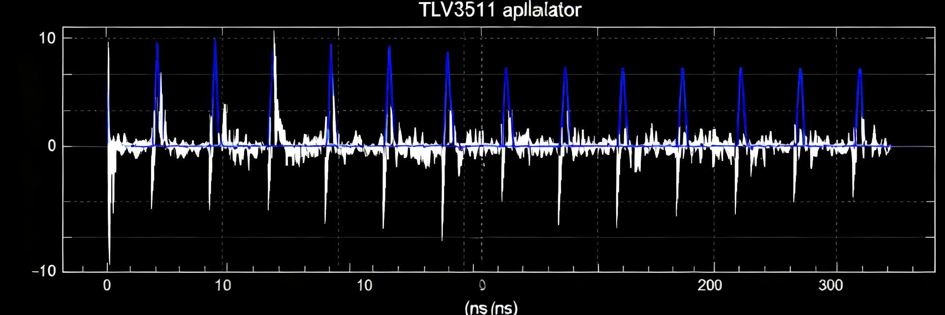
Key electrical specifications
Point: Key electrical numbers define suitability for low-power, high-speed designs. Evidence: Typical spec set includes supply range, propagation delay, input common-mode, output stage, supply current, offset, hysteresis, and output drive. Explanation: A compact spec table below highlights the metrics engineers read first when comparing comparators for timing-critical or battery-conscious systems.
| Parameter | Typical / Range |
|---|---|
| Supply voltage (Vcc) | 1.8 V – 5.5 V |
| Propagation delay (tpd) | ~6 ns (typ), ≤10 ns (max) |
| Input common‑mode | Rail‑to‑rail (including Vcc and GND margins) |
| Output stage | Push‑pull (no external pull‑ups needed) |
| Quiescent current | Low µA range per channel |
| Input offset (V) | ± a few mV (typ) |
| Hysteresis | Small, device dependent |
| Output drive | Drives standard CMOS loads; VOH/VOL vs RL indicated in datasheet |
| Package / pins | Small SOT‑/SC‑style packages, 5–8 pins typical; low footprint |
| Thermal notes | Surface mount thermal path; keep PCB area for dissipation |
Recommended quick-read bullets for datasheet scanning
Point: Engineers need a rapid checklist for datasheet triage. Evidence: Common failure to match test conditions causes misleading comparisons. Explanation: Use the checklist below when scanning timing and power sections to ensure apples-to-apples comparison.
- Must‑check test conditions: VCC, RL, CL, input slew rate and ambient temperature; timing tables often list conditions that materially affect tpd.
- Compare VOH/VOL vs. RL at the same supply voltage and load; note output stage (push‑pull vs. open‑drain).
- Confirm input common‑mode limits and required headroom for signals near rails.
- Scan for internal pull devices or references that change bias and quiescent current under load.
Performance Benchmarks & Measured Behavior — TLV3511QDCKRQ1 in real tests
Propagation delay, rise/fall times and timing jitter
Point: Reproducible timing data requires strict test conditions. Evidence: Measure at VCC values (e.g., 3.3 V and 5 V), with defined input slew (e.g., 1 V/ns) and load (RL = 10 kΩ, CL = 10 pF). Explanation: Use a 500 MHz+ oscilloscope, short ground spring/probe, and differential measurement across output to minimize probe-induced error; report mean, standard deviation, and worst‑case tpd across multiple units and temperatures.
Power, input common‑mode and output drive under load
Point: Supply current and drive capability shift with switching rate and load. Evidence: Measure quiescent current at idle and switching currents at representative toggle rates (kHz→MHz). Explanation: Plot supply current vs. switching rate and VCC; characterize VOH/VOL into RLs (1 kΩ, 10 kΩ) to quantify timing shift under load and ensure the comparator meets system timing at intended drive conditions.
Head-to-Head: How TLV3511QDCKRQ1 compares to peer comparators
Strengths — where it outperforms
Point: The part balances speed, low idle current, and small package. Evidence: Single‑digit‑ns tpd with µA‑range quiescent current and rail‑to‑rail inputs reduces BOM and board area. Explanation: For space‑constrained, battery‑sensitive systems requiring fast threshold detection, its push‑pull output avoids external pull‑ups and simplifies logic interfacing to CMOS without extra components.
Trade‑offs and limits to watch
Point: No single part is optimal for every use‑case. Evidence: Potential limits include limited built‑in hysteresis, absence of an explicit shutdown pin, and moderate output drive vs. dedicated drivers. Explanation: Prefer this comparator when speed and low idle power are primary; choose alternatives if large hysteresis, rail‑to‑rail drive into heavy loads, or a shutdown feature are essential.
Design & Integration Guide — practical application patterns
Typical circuit topologies and use cases
Point: Three compact topologies cover most applications. Evidence: (1) Single‑ended threshold: comparator input through 10 kΩ divider and 1 MΩ pull‑down, output to logic. (2) Window detection: two comparators with reference ladder (10 kΩ series resistors) and small hysteresis network. (3) Push‑pull drive to CMOS: keep series input resistor 50–200 Ω and add 10 pF to tame ringing. Explanation: Expected signal levels are rail‑to‑rail for inputs; timing budgets should account for 6–10 ns tpd plus propagation through any RC filtering.
PCB layout, decoupling and input protection best practices
Point: Layout and protection affect measured speed and stability. Evidence: Use a 0.1 µF decoupling cap within 2 mm of VCC–GND pins and a 10 nF local cap for high‑frequency transients; keep input traces short and provide solid return paths. Explanation: Add series resistors (50–200 Ω) or small RC filters to prevent oscillation on high‑bandwidth inputs; clamp diodes or TVS for harsh environments, balancing protection capacitance to avoid slowing input edges.
Bench Test & Validation Checklist — tests every engineer should run
Recommended test setup and step‑by‑step measurements
Point: A repeatable plan reduces variance between labs. Evidence: Use fixture with short wiring, regulated supplies with low noise, a 1 GHz+ pulse generator for input edges, and an oscilloscope with >500 MHz bandwidth. Explanation: Steps: verify static thresholds → measure tpd at multiple VCCs and input slew rates → measure supply current idle vs. switching → perform temperature sweep (−40 °C to +85 °C) to qualify behavior in target environment.
Pass/fail criteria, common failure modes and troubleshooting
Point: Define acceptance thresholds tied to system requirements. Evidence: For logic interfacing, require tpd ≤ 10 ns and VOH/VOL meeting logic thresholds at specified RL; for pulse detection, require jitter < specified fraction of pulse width. Explanation: If failures occur, check probe loading, layout parasitics, input slew, unintended hysteresis, and decoupling; swapping to shorted test wiring often reveals layout‑induced issues.
Summary
- The TLV3511QDCKRQ1 provides a compelling balance of single‑digit‑nanosecond responsiveness and low quiescent current, making it a strong choice for space‑constrained, low‑power timing and threshold applications where comparator speed and power both matter.
- Key specs to verify during selection include propagation delay vs. VCC and input slew, rail‑to‑rail input behavior, output drive into target RL, and quiescent current at expected temperature and switching rates.
- Use the provided bench checklist and integration patterns—short decoupling paths, series input resistors, and controlled input slew—to reproduce specs and ensure reliable system performance.
FAQ
How does the TLV3511QDCKRQ1 compare in propagation delay to other comparators?
The TLV3511QDCKRQ1 typically achieves single‑digit‑nanosecond propagation delays (around 6 ns typ), which is competitive for the class when measured under matched conditions (specified VCC, RL, CL, and input slew). For fair comparison, ensure identical test setup and report distributions across multiple units.
What test conditions should I standardize when characterizing a comparator?
Standardize VCC, ambient temperature, RL, CL, and input edge slew rate. Use a high‑bandwidth oscilloscope, minimize probe ground loop, and report mean and worst‑case tpd across several samples. Also log supply current at idle and under switching to capture dynamic power behavior.
When should I avoid using this comparator and pick a different spec set?
Avoid this class if your application demands built‑in wide hysteresis, a hardware shutdown pin, or very high output drive into heavy loads without buffering. If the system requires strong drive into 50 Ω loads or large hysteresis for noisy thresholds, select a comparator or driver tailored to those needs.
What PCB layout practices prevent oscillation in the TLV3511QDCKRQ1?
To prevent oscillations, place a 0.1 µF ceramic decoupling capacitor within 2 mm of the VCC pin, keep signal traces as short as possible to minimize parasitic capacitance, and isolate input lines from high-speed output nodes with guard traces or a continuous ground plane.