
The TLV3232DSGR datasheet frames a comparator that targets low-power, fast threshold detection: bench and datasheet figures indicate roughly 20–25 ns propagation delay, a typical PSRR near 90–92 dB across supply, and quiescent current of a few hundred microamps per channel. This introduction links those headline metrics to practical design questions — how PSRR and propagation delay manifest on the bench, and which trade-offs you must manage to get datasheet-like behavior in a real system.
This deep-dive is organized as a checklist and how‑to guide: at-a-glance specs, full-spec walk-through, PSRR and timing analysis, practical circuits, and repeatable bench procedures. Readers will find compact tables and specific test steps that let you validate the device in a 5 V or lower rail environment with typical lab equipment and layout constraints in mind.
TLV3232DSGR datasheet — Background & at-a-glance specs
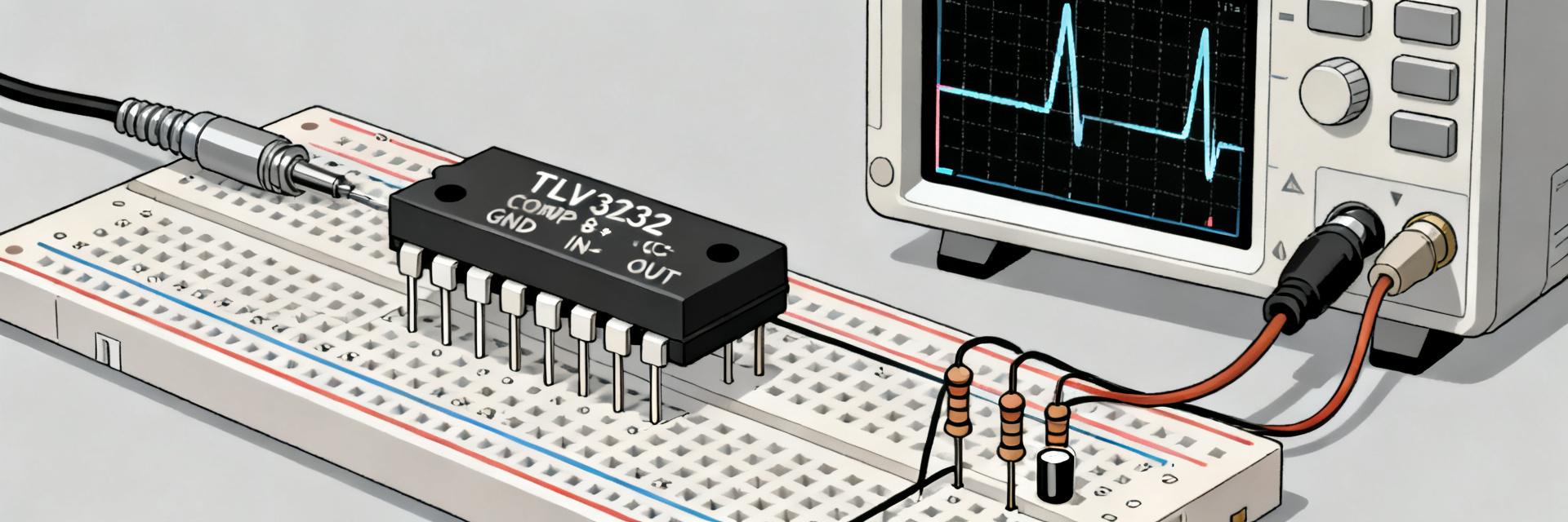
What the TLV3232DSGR is (device family snapshot)
The TLV3232DSGR datasheet presents a low‑power, high‑speed rail‑to‑rail‑input comparator with a push‑pull output intended for fast threshold detection in battery‑sensitive systems. In short: small package, low quiescent current, and short propagation delays make it suitable for wake‑on‑signal and fast-event capture tasks where supply budgeting and timing matter.
- Supply range: 1.8 V to 5.5 V (recommended operating window).
- Typical quiescent current: ~150–300 µA per channel depending on VCC.
- Typical propagation delay: ~20–25 ns (depends on overdrive and CL).
- Typical PSRR: ~90–92 dB at low frequencies (roll-off with frequency).
- Temp range, hysteresis, and package options: see recommended operating conditions and SOT/SOIC variants.
Key numbers to watch (mini spec table + how to read them)
Below is a compact selection of datasheet values you should extract for system budgeting; each entry notes typical test conditions that determine reported values and how to interpret them against system loads and noise sources.
| Parameter | Typical / Remark |
|---|---|
| VCC range | 1.8 V – 5.5 V (operate within recommended window) |
| Iq per channel | ~150–300 µA (typ depends on VCC) |
| Propagation delay (tPLH/tPHL) | ~20–25 ns typical (measured at specified overdrive, CL) |
| PSRR | ~90–92 dB typical (low‑freq, falls with frequency) |
| CMRR | Specified at DC/low freq; influences differential noise immunity |
| Hysteresis | Small built‑in or configurable; affects chatter and timing |
| Output drive | Push‑pull, source/sink limits depend on VCC and package |
| Absolute max | Voltage and input protection limits; do not exceed |
When reading the table, note each typical value is tied to conditions (VCC, RL, CL, 25°C). For system predictions, adjust for worst‑case temp, higher CL, and supply droop rather than relying solely on typ values.
TLV3232DSGR datasheet: Full specs walkthrough (datasheet checklist)
Electrical characteristics explained — which rows matter most
Prioritize DC bias (Iq), input common‑mode range, output drive, and AC timing (tPLH/tPHL). For each row, confirm the measurement conditions: VCC value, load resistor RL, load capacitance CL, and temperature. For example, propagation delay reported at a given overdrive and CL will lengthen with larger CL or lower VCC; similarly, output swing vs load affects logic margins at the receiving stage.
Absolute max & recommended operating conditions — design limits
Respect absolute maximum supply voltages and input pin limits to avoid irreversible damage. Use the recommended operating window for derating: allow margin for transient spikes and thermal increases, and follow package soldering limits. Verify ESD and handling notes before prototyping; these items are commonly overlooked and cause early failures in evaluation boards.
PSRR Deep-Dive: why ~90–92 dB matters in real circuits
PSRR explained and how it’s measured
PSRR (Power‑Supply Rejection Ratio) quantifies how supply ripple couples into the comparator output. Typical measurement injects a small AC ripple onto VCC while driving a known input and measuring output amplitude vs frequency. The datasheet’s PSRR curve shows high rejection at low frequency and a roll‑off as the device internal nodes and decoupling capacitors become less effective.
Practical impact & design tips to maximize effective PSRR
Effective PSRR directly influences output jitter and noise when supply ripple exists. To preserve the quoted ~90 dB, use a 0.1 µF ceramic close to VCC pin plus a 1 µF bulk cap within 5 mm, minimize series inductance on the supply, place ground returns carefully, and consider a small series resistor or ferrite for switching rails. Verify with injected ripple tests across frequency to validate layout choices.
Propagation delay & timing analysis (20–25 ns behavior)
Understanding propagation delay, sources of variation
Propagation delay (tPLH/tPHL) is time from input threshold crossing to output transition. It varies with supply voltage, CL, input overdrive, temperature, and lot‑to‑lot manufacturing spread. Datasheet “typ” values assume specific overdrive and CL; use “max” numbers for worst‑case timing budgets and include margin for measurement and environmental variation.
Measuring and optimizing delay — bench setup & practical tweaks
Use a fast pulse generator, a scope with >200 MHz bandwidth, and proper probe compensation. Drive the comparator with a clean edge, measure at the device output with minimal probe capacitance, and record tPLH/tPHL across VCC and CL conditions. To optimize, reduce CL, avoid long traces, use proper pull resistors, and ensure stable supply decoupling.
Design & application guidelines — typical circuits and trade-offs
Typical application circuits and configuration notes
Example 1: Fast threshold detector with minimal hysteresis — use small input resistor, direct coupling, and minimal added capacitance; expect fastest edges but potential chatter. Example 2: Small intentional hysteresis — add a feedback resistor network to create ~10–50 mV hysteresis, improving noise immunity at modest cost in propagation time. In both, decoupling of 0.1 µF + 1 µF and pull resistors 10 kΩ–100 kΩ are sensible starting ranges.
Trade-offs: speed vs power vs noise (how to choose for your system)
If you need sub‑25 ns response, favor higher VCC within the recommended range and minimize CL; expect Iq toward the higher end. If lowest power is required, accept longer delays and validate PSRR impact on jitter. Use a simple decision matrix: prioritize speed for event capture, prioritize power for always‑on sensing, and validate PSRR if supply switching is nearby.
Testing, validation & troubleshooting checklist (hands-on)
Bench tests to validate datasheet claims (PSRR, propagation delay, CMRR)
Equipment: fast pulse generator, 200+ MHz scope, AC source or function generator for ripple injection, precision probes. Test steps: measure tPLH/tPHL at specified VCC and CL, inject supply ripple and record output amplitude vs frequency, and measure common‑mode response. Record results in a simple table and compare to datasheet typical and max values, allowing a margin of ~10 dB for PSRR at low freq.
Common failure modes and fixes
Frequent issues: poor decoupling, long traces adding CL, probe loading, wrong reference levels, and thermal shifts. Fixes: move caps closer, shorten traces, use lower‑capacitance probes, verify thresholds with a calibrated source, and run tests at elevated temperature to observe derating effects.
Summary
The TLV3232DSGR datasheet highlights a fast, low‑power comparator characterized by ~20–25 ns propagation delay and ~90–92 dB typical PSRR; translating those numbers to reliable system performance requires careful decoupling, control of load capacitance, and disciplined measurement technique. Use the tables and bench procedures above to validate performance and apply layout and filtering tips to approach datasheet results in real products.
Key takeaways
- TLV3232DSGR performance depends on VCC, CL and overdrive — validate tPLH/tPHL across conditions before integration.
- PSRR ~90–92 dB at low frequencies reduces supply‑induced jitter, but layout and decoupling are critical to preserve it.
- For fastest response, minimize CL and place decoupling within ~5 mm of VCC pin; use typ/max margins in timing budgets.
- Bench validation requires a fast scope, ripple injection for PSRR, and repeatable probe practices to avoid measurement artifacts.
Frequently Asked Questions
How does TLV3232DSGR propagation delay vary with supply?
Propagation delay shortens with higher VCC within the recommended range and grows with larger CL or lower input overdrive. Measure tPLH and tPHL at multiple VCC points and include the worst‑case (max) datasheet numbers plus safety margin in timing budgets to ensure reliable system timing.
What PSRR behavior should be expected for the TLV3232DSGR?
Expect strong rejection (~90 dB) at low ripple frequencies and a roll‑off as frequency increases; effective PSRR in a board depends on decoupling and layout. Validate by injecting AC ripple onto VCC while keeping input conditions fixed and measuring output modulation across frequency.
What bench setup yields repeatable propagation delay measurements?
Use a clean pulse source with fast edges, a scope with sufficient bandwidth (>200 MHz), minimal probe capacitance, and consistent loading (specified CL). Trigger on the input edge and measure output crossing times; repeat across temperature and supply points for full characterization.
How do you minimize output jitter and maintain high PSRR in your layout?
To preserve the ~90-92 dB PSRR, place a 0.1 µF ceramic capacitor close to the VCC pin alongside a 1 µF bulk capacitor within 5 mm, minimize series inductance on the supply rail, and route ground returns cleanly.