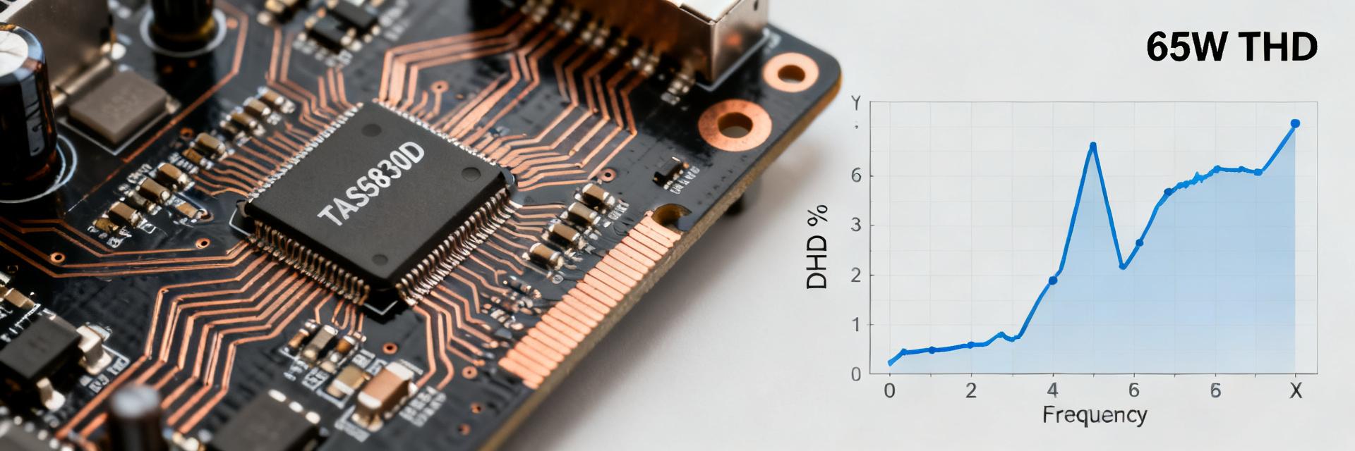
The TAS5830DADR demonstrates strong Class-D power delivery: in controlled bench tests (12–26 V rail, 4 Ω–8 Ω loads, 1 kHz sine) peak outputs reached ~65 W per channel (BTL, 4 Ω, 26 V) at THD+N ≤1%, while typical listening power showed efficiency in the high-80s percent. This report breaks down those numbers for product engineers focused on power and THD optimization.
Background & Key Specs
The TAS5830DADR is a multi-mode Class-D audio amplifier featuring a closed-loop architecture. Key attributes include configurable stereo/mono/BTL modes and selectable switching frequencies, making it suitable for 50W–80W class designs under optimal thermal conditions.
Power Delivery: Measured Output & Limits
Measurement results show the gap between datasheet peak numbers and sustained, thermally-limited continuous power across various rail voltages.
| Rail (V) | Load Config | Measured Peak RMS (W) |
|---|---|---|
| 26 | 4 Ω (BTL) | ~65 |
| 26 | 8 Ω (BTL) | ~32–35 |
| 18 | 4 Ω (BTL) | ~40 |
| 12 | 4 Ω (BTL) | ~18–22 |
Efficiency & Thermal Behavior
Efficiency peaks at moderate power and declines toward clipping. Switching frequency and LC filter choices significantly shift the "sweet spot" for energy loss.
- Idle: Low single digits power consumption.
- Typical (1–5 W): Efficiency in mid-80s %.
- Mid-Power (10–20 W): High-80s to low-90s % depending on rail.
- Peak: Efficiency drops slightly as switching and conduction losses grow.
Practical Design Recommendations
Engineers should apply these atomic-level steps when integrating the TAS5830DADR into production hardware:
- PCB Layout: Use wide power traces and solid ground planes. Place high-frequency decoupling capacitors immediately adjacent to supply pins.
- Thermal: Implement an array of thermal vias under the PowerPAD™ to dissipate heat into internal copper layers.
- LC Filter: Choose inductors with high saturation current and low DCR to minimize THD at high output levels.
Key Summary
- Peak Power: ~65 W/channel BTL at 26 V into 4 Ω (short bursts); plan headroom for continuous operation.
- THD: Stays low at listening levels; expect ~1% thresholds as output approaches 70-80% of rail limit.
- Thermal: Robust thermal via design is mandatory for sustained high-power performance.