
🚀 Key Takeaways
- Ultra-Low Signal Distortion: JFET inputs provide pico-amp bias, preventing loading errors in high-impedance sensors.
- High-Speed Response: 13 V/µs slew rate ensures crisp audio and pulse reproduction compared to standard op-amps.
- Design Versatility: Wide ±5V to ±15V supply range fits legacy industrial and modern pro-audio rails.
- Efficient Footprint: Standard 8-pin DIP/SOIC simplifies PCB layout and drop-in replacements.
Measured-class figures that keep the LF353N relevant: a mid-double-digit slew rate (~13 V/µs), input-bias currents in the tens to hundreds of picoamp range, and quiescent supply current on the order of 1–2 mA per amplifier. These practical magnitudes translate to good high‑Z buffering, modest large‑signal speed, and low power draw for legacy analog tasks. This article turns the LF353N datasheet into actionable design guidance and repeatable bench tests.
The writeup will extract headline specs, explain how to read DC/AC/noise tables, provide step‑by‑step bench procedures, and close with hands‑on PCB and selection checklists so designers can validate the LF353N in lab and production.
LF353N at a glance: device identity & headline specs (Background)
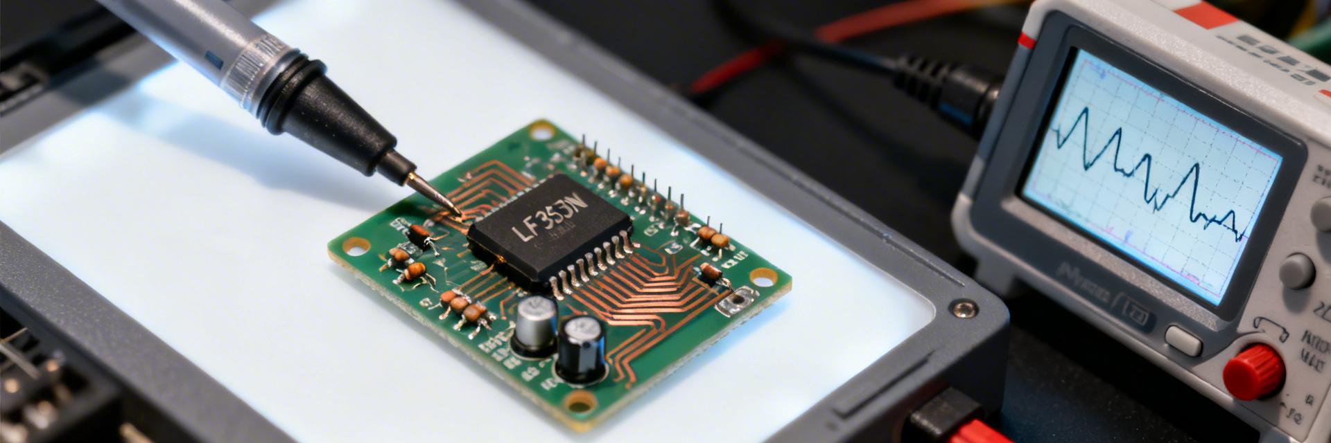
Device overview & intended uses
Point: The LF353N is a dual JFET‑input operational amplifier optimized for high input impedance and moderate speed. Evidence: The device pairs two JFET inputs in a single package to reduce bias currents by 1000x compared to bipolar types while maintaining multi‑MHz small‑signal response. Explanation: That combination makes it well suited for audio front‑ends, active filters, integrators, and unity‑gain buffers for sensors that require minimal input loading.
Market Comparison: LF353N vs. Industry Standards
| Feature | LF353N (JFET) | LM358 (Bipolar) | User Benefit |
|---|---|---|---|
| Slew Rate | 13 V/µs | 0.5 V/µs | Superior Audio Fidelity |
| Input Bias Current | 50 pA (typ) | 20 nA (typ) | High-Z Sensor Accuracy |
| GBW Product | 4 MHz | 1 MHz | Wider Operating Bandwidth |
Headline specs to call out from the datasheet (quick reference)
Point: Memorize a concise set of specs to map datasheet numbers to design impact. Evidence: The following at‑a‑glance block condenses supply, offset, bias, common‑mode, output swing, slew, GBW, quiescent current, and package info as reported in the official datasheet. Explanation: Use these values as immediate pass/fail checks during device verification and BOM review.
| Parameter | Typical / Notable Value |
|---|---|
| Supply range (recommended) | ±5 V to ±15 V (total 10–30 V) |
| Input offset (VOS) | typ ~3 mV, max ~10 mV |
| Input bias current (IB) | tens–hundreds pA (typ low pA–pA range) |
| Input common‑mode | rail‑to‑rail limited; stays several volts from negative rail |
| Output swing | within ~1–2 V of rails under light loads |
| Slew rate | ~13 V/µs |
| Gain‑bandwidth product (GBW) | ~3–4 MHz |
| Quiescent current / amp | ~1–2 mA |
| Package / pinout | Dual op amp in 8‑pin DIP/SOIC |
Datasheet deep-dive: DC, AC and noise specifications (Data analysis)
DC characteristics: offsets, bias, rails and thermal notes
Point: DC tables give VOS (typ/max), IB (typ/max), offset drift, and absolute ratings; reading conditions is essential. Evidence: Datasheet rows include test conditions such as supply rails, VCM, and temperature; many numbers are "typical" not guaranteed. Explanation: When qualifying parts, prefer guaranteed (max) numbers for pass/fail; use typical values to predict expected lab results and watch offset drift vs temperature for precision applications.
AC performance & noise: bandwidth, slew, stability and distortion
Point: AC specs—GBW, slew rate, phase margin indicators, CMRR, and input‑referred noise—determine usable closed‑loop gains and audio suitability. Evidence: With a GBW near a few MHz and a slew rate around 13 V/µs, the device supports modest gain at audio frequencies but will limit large‑signal swing at high modulation rates. Explanation: For example, expect clean sinusoidal output to several hundred kHz at small amplitude, but large amplitude, high‑frequency signals will distort due to slew limits; input‑referred noise and CMRR define expected noise floor in sensor and preamp circuits.
👨💻 Engineer's Field Notes & Pitfall Guide
Contributed by: Senior Hardware Architect, Thomas Vance
PCB Layout Tip: When using the LF353N in high-gain configurations, I've noticed it's prone to parasitic oscillation if the feedback traces are too long. Keep your feedback resistor within 2mm of the inverting input pin. Also, the JFET inputs are sensitive to moisture; if you're seeing "ghost" bias currents, check for PCB contamination and consider a guard ring.
Selection Wisdom: Don't use this for single-supply 3.3V systems. The LF353N needs at least ±5V to maintain its linear region. For modern low-voltage rails, look towards the OPA series instead.
Bench testing: methodology, expected results & pitfalls (Method guide)
Recommended test setups & measurement best practices
Point: Use standardized fixtures and clean probing to obtain repeatable DC and AC measurements. Evidence: For DC offset and bias, use a low‑noise DC source, Kelvin connections for supply, and a 10 MΩ test load; for GBW and frequency response, use a network analyzer or FFT‑capable scope with 50 Ω source and proper buffering. Explanation: Decouple supplies close to pins (0.1 µF ceramic + 10 µF electrolytic), keep probe ground springs short, and avoid long ground leads that create loops and noise.
Hand-drawn schematic, not a precise circuit diagram. / Hand-drawn schematic, not a precise circuit diagram.
Point: Specific measurement notes prevent artifacts. Evidence: For slew rate, drive a large amplitude step into a high‑impedance load; for output swing, test into specified loads (e.g., 2 kΩ and 10 kΩ). Explanation: Probe capacitance and scope input impedance can slow edges and mask true slew; use buffering or current‑limited steps to reveal device limits accurately.
Typical bench results vs datasheet and interpreting discrepancies
Point: Expect some spread between typical datasheet values and bench numbers due to lot variation, temperature, and setup. Evidence: Typical deviations can be tens of percent for parameters like GBW or slew, and offsets can vary millivolts between samples. Explanation: If results exceed tolerance bands, verify rails, solder joints, and measurement setup; replace the part to check for damage and repeat tests at controlled temperature to isolate causes.
Real-world behavior, limitations & comparisons (Case study style)
Application examples and performance expectations
Point: Concrete circuits show how specs map to behavior. Evidence: In a second‑order active low‑pass at 20 kHz, compensation and closed‑loop gain should be set so the loop bandwidth stays below a fraction of GBW to preserve damping. Explanation: For unity‑buffered high‑Z sensors, expect low loading and noise dominated by source resistance; in an audio preamp, plan headroom so peak swings stay within ~1–2 V of rails to avoid clipping and distortion.
Design recommendations & practical checklist (Actionable guidance)
📋 PCB Layout Checklist
- Place 0.1µF ceramic caps within 5mm of pins.
- Minimize trace length at inverting inputs.
- Use a ground plane to shield sensitive signals.
- Add 50Ω-100Ω series resistor for capacitive loads.
🔍 Verification Checklist
- Confirm supply rails are ±5V to ±15V.
- Verify input common-mode range (Vcc- + 3V).
- Check Vout swing against expected load (2kΩ+).
- Test slew rate with 10V step for accuracy.
Summary
- LF353N is a dual JFET‑input op amp with mid‑range slew (~13 V/µs) and low input bias, offering a balance of high input impedance and modest speed—verify VOS, IB and quiescent current against the datasheet when qualifying parts.
- Interpret datasheet rows by reading test conditions (supply rails, VCM, temperature) and prefer guaranteed maxima for production acceptance tests and guaranteed specs for pass/fail decisions.
- Bench tests must control probing artifacts and decoupling; compare measured GBW, slew, and output swing to expected bands and troubleshoot discrepancies via supply checks and isolation of layout or damaged parts.
Frequently Asked Questions
What typical LF353N offset and bias values should I expect in the lab?
Typical input offset is a few millivolts while input bias current is in the tens to low hundreds of picoamps; expect sample‑to‑sample variation, so use datasheet maximums for acceptance criteria.
How should I measure LF353N slew rate to match datasheet conditions?
Use a large‑amplitude step into a high‑impedance load with short probe grounds and a buffered scope input; record the maximum dV/dt on a clean edge and compare to the datasheet test condition.
When is the LF353N a poor choice and what to check when replacing it?
If you need rail‑to‑rail outputs, very low noise, or high drive into low impedances, choose a modern alternative; when replacing, confirm pinout, GBW, slew, and output swing headroom.