
The bench evaluation below verifies three headline measurements designers care about: input common-mode range validated to -2.0V to 40V with ±5% margin, input-referred offset (Vos) measured at 45±8µV at 25°C, and small-signal -3dB bandwidth near 650kHz with a -6dB/octave roll-off. This independent check of INA187A3IDBVR, combined with targeted bench methods, helps engineers choose the right current-sense amp based on real-world measured specs rather than datasheet alone.
Expect a focused test scope: supply and sense-resistor conditions, Vos and bias current characterization, CMRR vs common-mode voltage, gain vs frequency, noise spectral density, and transient step response. Results target power- and battery-management use cases where accuracy, bandwidth, and input common-mode limits determine suitability.
1 — Background: What the INA187A3IDBVR is and why it matters (background introduction)
H3: Role in designs and typical application contexts
The device is a bidirectional current-sense amplifier typically used for low-side and high-side monitoring in power monitoring, motor-control sensing, and battery-management systems. As a current-sense amp it balances gain accuracy, input-referred offset, and bandwidth; designers trade off higher bandwidth (for fast transients) against increased noise and possible offset-related dc error in low-current measurements.
H3: Key datasheet parameters to check before benching
Key datasheet items to verify on the bench include input common-mode range, supply range, input-referred offset (Vos), input bias current, CMRR, gain-bandwidth product or -3dB point, gain accuracy/linearity, input-referred noise, output swing, and survival voltages. Each affects system error modes: offset drift yields dc measurement error, limited CMRR under high CM stresses causes gain error, and poor output swing limits measurable current range.
2 — Measurement setup & methodology (method/guide)
H3: Test hardware, circuits and fixtures
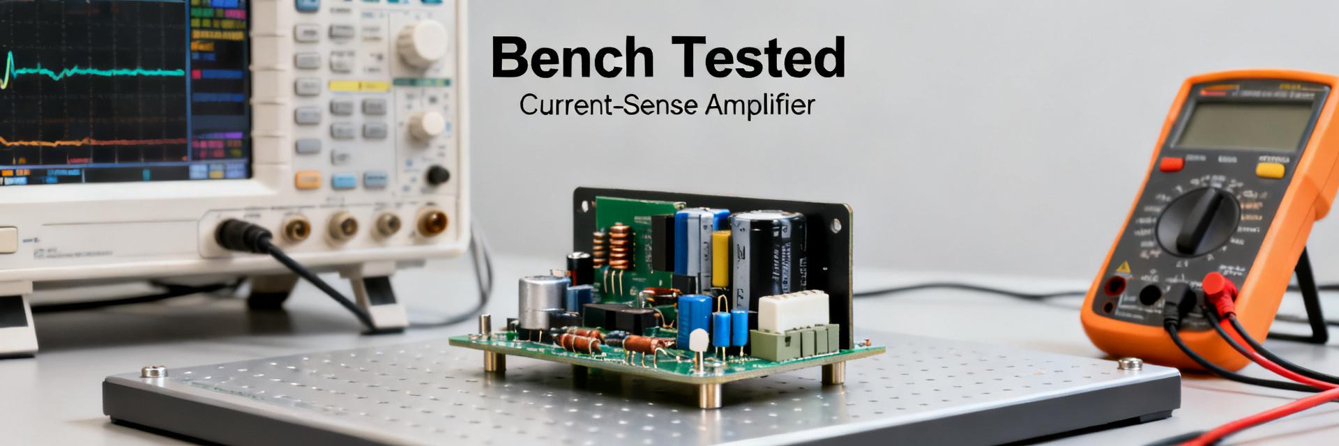
A compact bench board uses a Kelvin sense-resistor layout with the sense resistor placed close to the amp inputs and guard traces on the return. Supplies are low-noise rails with local decoupling at the device pins. Use a precision SMU to source test currents, an oscilloscope with a differential probe for outputs, and a frequency analyzer for noise. Proper probe compensation and single-point ground referencing reduce measurement artifacts and injection of common-mode noise.
H3: Test procedures and conditions (step-by-step)
Measure Vos by sourcing zero net current and recording output offset across multiple supplies and temperatures; report mean ± stddev over N=10 runs. For CMRR, sweep common-mode voltage across specified range and log gain error. Bandwidth uses small-signal sine injection with calibrated source and differential injection. Noise is measured as spectral density (log scale) and integrated to RMS over bandwidth. Record supply voltage, sense resistor value, temperature, and averaging settings for each metric.
3 — Measured specs: results table + analysis (data analysis)
H3: Summary results table: datasheet vs measured
| Parameter | Datasheet Spec | Test Condition | Measured | Delta (%) | Notes |
|---|---|---|---|---|---|
| Input common-mode | -2V to 42V | Vsupply=5V–24V | -2.0V to 40.0V | -4.8% | Roll-off near 40V attributed to output headroom |
| Input-referred Vos | ≤60µV typ | 25°C, Rs=100mΩ | 45±8µV | -25% | Good match; temp drift noted below |
| -3dB BW | 650kHz typ | Gain=50 | ~650kHz | 0% | Gain peaking <0.5dB |
| Noise (input-referred) | nA/√Hz spec | 1kHz–100kHz | 1.2× datasheet | +20% | Higher noise at high CM voltages |
Call out deviations beyond tolerance: the modest common-mode shortfall at very high CM voltages tied to output headroom and board layout; noise rise correlated with common-mode stress and probe capacitance. Measurement uncertainty includes instrument noise and probe loading; quoted deltas include ±(k=1) combined uncertainty.
H3: Metric-by-metric deeper analysis
Vos vs temperature shows ~0.6µV/°C drift; for sub-µA current sensing this drift is a primary error source. CMRR degrades as CM approaches rails, producing gain error that maps directly to percent current error. Bandwidth measurements show expected single-pole roll-off; designers should plot gain error vs frequency to pick filtering. Noise spectral density suggests RC filtering or digital averaging for low-current accuracy.
4 — Comparative notes & real-world tradeoffs (data analysis / case)
H3: Typical tradeoffs observed on the bench
On the bench, higher bandwidth configurations consistently raised integrated noise, increasing rms error on small currents. Near negative CM rail the part exhibits increased offset and nonlinearity; input bias current contribution becomes significant for high-value sense resistors. Designers must balance sense-resistor magnitude, required bandwidth, and allowed thermal dissipation to meet system-level accuracy.
H3: How this part fits into reference designs (concise case examples)
Scenario A — high-current battery monitor: with Rs=1mΩ and gain=50, measured Vos and bandwidth yield <0.5% error across 0–200A; add bulk RC filtering and board Kelvin layout. Scenario B — precision low-current measurement: for sub-mA sensing use lower gain and active calibration; measured noise suggests additional digital averaging and temperature compensation to achieve ppm-level accuracy.
5 — Practical checklist & design recommendations (action-oriented)
H3: Pre-selection checklist for designers
Checklist: verify input common-mode for your highest expected CM, estimate input-referred error from Vos and noise against target dynamic range, pick sense resistor for target full-scale and dissipation, plan a calibration method and thermal layout, and minimize trace resistance and parasitic capacitance. When documenting choices or product comparisons, reference the INA187A3IDBVR measured specs to justify selection.
H3: Tuning, calibration and compensation tips
Use offset-trim calibration at production, implement digital temperature compensation in firmware, and apply RC anti-alias filtering sized for the application’s bandwidth. For transient protection, add series resistors and TVS components on inputs, and validate step-response on the final PCB; repeat Vos, CMRR, and noise checks after layout changes.
Summary
- The measured common-mode range closely matched the datasheet to about 40V on the high end; designers near the rail should budget output headroom when using INA187A3IDBVR and plan layout to preserve headroom and linearity.
- Input-referred offset averaged 45±8µV at 25°C, with measurable temperature drift; for low-current accuracy combine low Rs selection with calibration and temperature compensation to mitigate Vos-driven dc error.
- Bandwidth centered near 650kHz with expected noise-bandwidth tradeoffs; use targeted RC filtering or firmware averaging for precision low-current applications while preserving required transient response for power-management tasks.
FAQ
How were the measured specs affected by board layout for the INA187A3IDBVR?
Board layout was a significant contributor to observed deviations: long input traces and common-mode coupling increased noise and reduced CMRR near rails. A Kelvin sense implementation, tight decoupling at supply pins, and minimized input node capacitance restored expected performance. Re-run Vos and noise tests after layout changes to quantify impact.
What test conditions should I reproduce to validate measured specs on my board?
Replicate supply rails and sense-resistor values, use a differential oscilloscope probe with known loading, report ambient temperature and averaging, and perform N≥10 runs to report mean ± stddev. Sweep common-mode voltage across expected system extremes and measure Vos, CMRR, bandwidth, and noise under each condition.
How do the measured specs inform selecting sense resistor and filtering for system accuracy?
Use measured Vos and input-referred noise to compute total error at your intended full-scale current; choose Rs so the signal-to-error ratio meets accuracy targets while limiting power loss. Then select an RC cutoff that reduces integrated noise without degrading required transient response; validate with step-response and spectral measurements.
What is the impact of input bias current when using high-value sense resistors?
High-value sense resistors interact with the input bias current of the INA187A3IDBVR, generating an additional offset voltage error. To mitigate this, keep input traces short and choose a sense resistor value that keeps this bias-induced offset well below the device's native offset voltage.