
The LM324N remains a go-to quad op-amp for general-purpose analog design thanks to a wide supply range, modest unity-gain bandwidth near 1 MHz, and high DC open-loop gain that supports simple precision tasks. This datasheet-driven overview translates headline numbers into actionable design decisions.
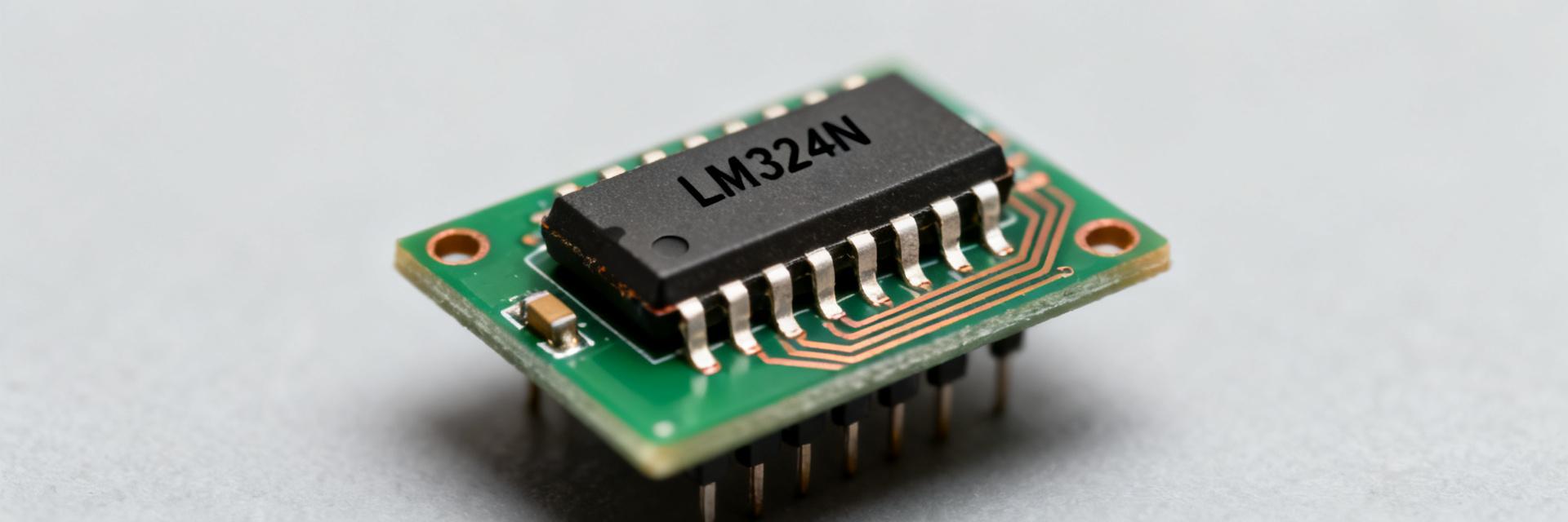
1. LM324N at a glance — datasheet essentials
Functional Description & Key Published Numbers
The datasheet defines four independent amplifiers optimized for single-supply operation. Before schematic entry, designers must log the absolute maximum ratings to ensure thermal and voltage compliance.
| Parameter | Typical Value | Unit | Conditions |
|---|---|---|---|
| Supply Voltage (Vs) | 3 to 32 | V | Single Supply |
| Unity-Gain Bandwidth | 1.0 | MHz | Vcc = 30V |
| Input Offset Voltage | 2.0 | mV | Ta = 25°C |
| Slew Rate | 0.5 | V/µs | RL ≥ 2kΩ |
2. Electrical characteristics — DC specs decoded
Input-related specs: Input offset voltage (Vio) and bias current (Ib) determine precision. The "LM324N input offset voltage typical" of 2mV is the benchmark for sensor front-ends. Note that offset can drift significantly across the operating temperature range.
Output and supply: Output swing relative to rails and quiescent current per amplifier set the headroom. For battery-powered applications, scale the ~0.7mA quiescent current by four to estimate total standby drain.
3. Dynamic performance & noise — AC specs
Translate the 1 MHz Unity-Gain Bandwidth (UGB) into closed-loop bandwidth. For a gain of 10, expect approximately 100 kHz of usable bandwidth. Slew rate (typically 0.5 V/µs) must be checked against required large-signal swing to prevent distortion.
4. Design Guidelines & Benchmarks
- Decoupling: Place 0.1 µF ceramic caps close to pins 4 and 11.
- Layout: Keep ground returns short and avoid high-impedance traces near inputs to minimize noise pickup.
- Stability: For capacitive loads >100pF, add a 50–100Ω series resistor at the output.
Frequently Asked Questions
How do I measure input offset accurately?
Use a low-noise short across the inverting and noninverting inputs, power the amp at the datasheet-specified Vs and temperature, and measure output with a high-resolution DMM. Convert output offset to input offset by dividing by the closed-loop gain; repeat at multiple temperatures to characterize drift.
What is a simple check for unity-gain bandwidth?
Configure a voltage follower on the bench, apply a small-amplitude sine, and sweep frequency until gain drops 3 dB. Ensure input amplitude stays within linear range and list Vs and load when reporting the measured unity-gain bandwidth.
Which decoupling values are recommended for stability and low noise?
Place a 0.1 µF ceramic capacitor close to power pins for high-frequency decoupling and a 1–10 µF bulk tantalum or electrolytic nearby for low-frequency stability. Tight ground returns and minimal trace inductance combine with decoupling to prevent oscillation.
What are common failure modes in LM324N designs?
If outputs rail unexpectedly, check input common-mode and supply rails; if oscillating, add output resistor or improve layout; swap packages to isolate assembly faults; verify supply decoupling and probe loading when diagnosing anomalies.
Conclusion: Prioritize supply range, input/output ranges, and bandwidth when choosing topology. Use the outlined bench validations to ensure performance matches published specs.