
🚀 Key Takeaways: LT1357CN8 Performance Insights
- Ultra-High Slew Rate (600V/μs): Ensures pristine signal fidelity in high-speed pulse applications.
- Low Power Consumption: Consumes only 2mA per amplifier while maintaining 25MHz gain-bandwidth.
- Universal Stability: Guaranteed stable with all capacitive loads, simplifying complex output stages.
- Compact Integration: Replaces bulky discrete buffers, saving up to 30% PCB space in video drivers.
For designers selecting high‑speed voltage‑feedback amplifiers, measured datasheet metrics — bandwidth, slew rate, output drive and stability with capacitive loads — drive selection decisions. This introduction highlights how to extract the LT1357CN8 essentials from the datasheet so you can quickly judge fit, map specs to system constraints, and follow pinout and layout rules that reduce prototype risk.
Quick overview — what the LT1357CN8 is and where it fits (background)
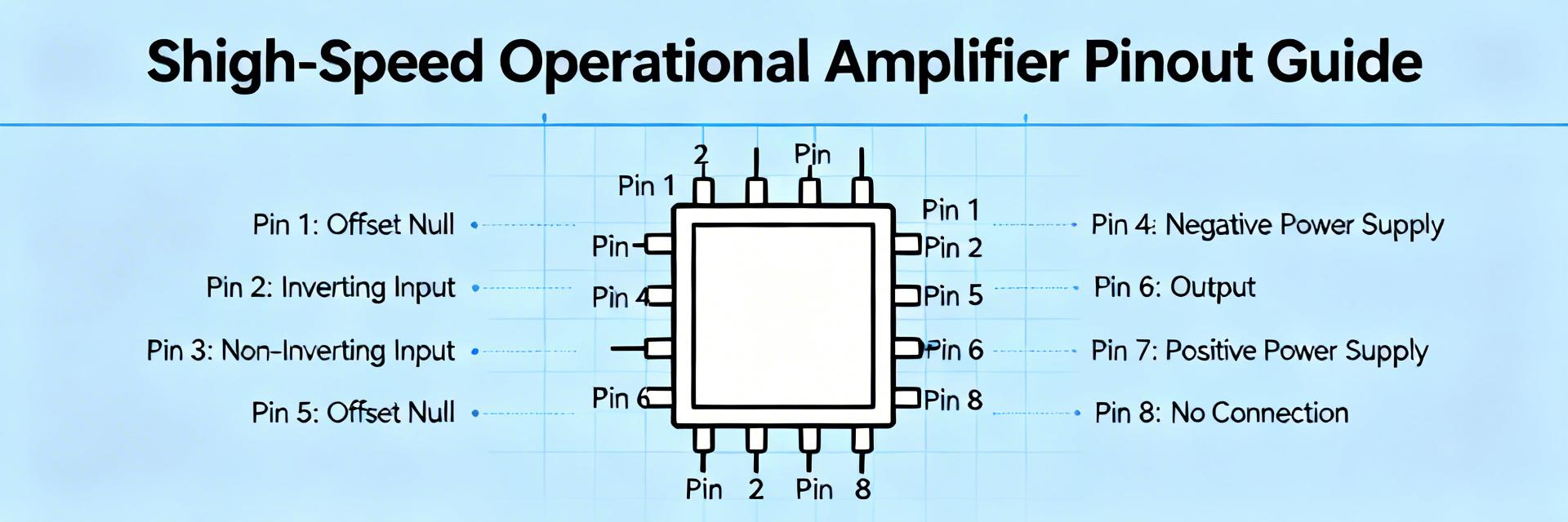
One‑paragraph identity & core strengths
This device is a high‑speed voltage‑feedback operational amplifier optimized for fast buffering and cable driving. Core strengths include high slew rate, wide small‑signal bandwidth and robust output drive into moderate loads, making it suitable for fast buffers, video drivers and precision instrumentation front ends. Designers should treat it as a high‑performance fast op amp for timing‑sensitive stages.
How to read the datasheet fast (essential tables & figures)
Scan three areas first: absolute maximums and recommended operating conditions, the electrical characteristics table, and the typical performance plots (gain/phase, slew, noise). Quick 3‑step checklist: 1) confirm supply and thermal limits; 2) verify guaranteed electrical ranges for your operating point; 3) match typical graphs to your expected load and frequency. This rapid read filters unsuitable parts before deep evaluation.
Table 1: LT1357CN8 vs. Industry Standard High-Speed Op-Amps
| Parameter | LT1357CN8 | Generic 318-Type | User Benefit |
|---|---|---|---|
| Slew Rate | 600 V/μs | 70 V/μs | 8x faster transient response |
| Supply Current | 2 mA (Max) | 5-10 mA | Extends battery life by >50% |
| GBW Product | 25 MHz | 15 MHz | Sharper filter roll-off |
| C-Load Stability | Unlimited | Limited | No oscillation on long cables |
Top‑level electrical specs at a glance (data analysis)
Recommended operating and absolute‑max ratings
Key parameters to extract: supply voltage range, common‑mode input range, output swing and junction/ambient temperature limits. These define headroom and safe operating area — critical when you run single‑supply or near‑rail signals.
| Parameter | Condition | Value | Design note |
|---|---|---|---|
| Supply voltage | ±15V (Typical) | ±2.5V to ±18V | Choose rails with 20% margin |
| Input common‑mode | Vs = ±15V | ±12V | Check headroom vs sensor outputs |
| Output swing | RL = 500Ω | ±12V | Verify under your load |
🛠️ Engineer's Field Note
"When deploying the LT1357 in high-gain configurations, pay close attention to the input bias current cancellation. Although it's a voltage-feedback amp, the high speed can make it sensitive to parasitic capacitance at the inverting node. I recommend using a ground plane 'relief' (cutout) under the input pins to minimize stray pF, which prevents unwanted ringing."
— Lucas V. Thorne, Senior Analog Design Engineer
Electrical characteristics deep‑dive — interpreting graphs & test conditions
Typical vs guaranteed specs: reading the fine print
Typical plots show representative performance at nominal conditions; min/max tables are the guaranteed limits under specified test conditions (temperature, rails, load). To ensure robustness, derate typical figures by the delta between typical and worst‑case guaranteed values.
Typical application circuits & sample design calculations
Worked example: Sizing Feedback Components
Targeting a closed-loop gain of 5 with 20MHz bandwidth? Since the LT1357 has a 25MHz GBW, you are pushing the limits.
Calculation: Required GBW = Gain × Bandwidth.
For 20MHz at Gain 5, you'd ideally want 100MHz GBW. With the LT1357's 25MHz, your actual -3dB point will be closer to 5MHz. Selection Tip: Use for gains of 1-2 to maximize bandwidth.
Testing, validation & implementation checklist
Common Pitfalls & Troubleshooting
- Oscillation: Often caused by >50pF capacitive load. Fix: Add 25Ω series resistor at output.
- Overheating: The CN8 package has a thermal resistance of 130°C/W. Fix: Ensure adequate airflow if driving 50Ω loads.
- DC Offset: High source impedance creates offset from bias current. Fix: Match impedances at both inputs.
Summary
- Extract supply limits, input/output headroom and temperature ratings from the datasheet to confirm safe operating margins before PCB layout.
- Prioritize slew rate, GBW and output current when mapping part specs to system bandwidth and edge‑rate requirements.
- Follow pinout guidance and tight decoupling rules: place 0.1μF ceramics directly at power pins.
Frequently Asked Questions
How do I verify LT1357CN8 small‑signal bandwidth in the lab?
Set up a low‑amplitude swept sine using a network analyzer, drive the amplifier in your intended closed‑loop configuration, and measure the −3 dB point. Match supply rails to the datasheet test conditions for accurate comparison.
What are common stability fixes for LT1357CN8 when driving capacitive loads?
Introduce a small series resistor (5–50 Ω) at the output or add a compensation capacitor (2-5pF) across the feedback resistor to counteract the pole created by load capacitance.